Laser techniques use a confocal microscopy platform with a laser source for the lighting and scanning of the sample area. It is possible in this way to image the die at high resolution through the silicon backside. Thanks to the interaction between the integrated circuit and the laser beam, it is possible to gather information on the component’s internal activity. Stimulation techniques: OBIRCh, OBIC, TLS, DLS, XVM Probing techniques: EOFM (LVI), EOP (LVP)
Laser
imaging
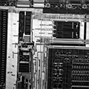
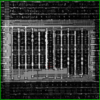
Backside imaging of a component through the silicon. It is possible in this way to visualize the active area of the component.
Laser
stimulation
The component can be locally perturbed by the laser beam. The analysis of the effects of the perturbation correlated to the laser position points to the weaknesses of the integrated circuit.
Short and open circuits localization. Parametrical Failure Analysis (soft defect) based on variation of: temperature, voltage, frequency, …
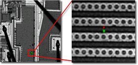
Laser probing
and frequency mapping
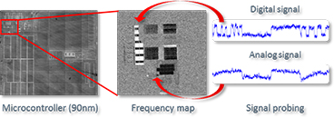
The laser beam can be used to measure the working frequency of each area of the component. Furthermore, it can be used in probing mode to get the internal signals waveforms.
Analysis of delay between signals,
Frequency anomalies detection,
Clock signal tree monitoring,
Memory descrambling
See below to find our other techniques